India’s Semiconductor Push: Defence Implications
- November 20, 2025 |
- Issue Brief
Summary
India’s semiconductor ecosystem faces systemic challenges that undermine defence modernisation and strategic autonomy. A defence semiconductor roadmap is required for India to address technological dependence and plug strategic vulnerabilities.
Introduction
Semiconductors constitute a strategic foundation of national security, technological capability and economic competitiveness. Their dual-use role spans civilian and defence applications, including space systems, secure communications and advanced radar technologies. At the core of every iPhone, email, photograph and YouTube video are the anonymous chips in the background.[1] Chip production remains heavily concentrated in a few countries, creating systemic vulnerabilities and opportunities for coercive leverage. Recognising these risks, India has launched the Indian Semiconductor Mission (ISM) under the Ministry of Electronics and Information Technology (MeitY). This initiative combines financial incentives, infrastructure development and international collaboration to build a resilient domestic ecosystem.[2] Achieving the objectives of this programme will be pivotal in establishing a viable industrial ecosystem. Yet, its significance extends beyond this, as it constitutes a critical defence requirement and a national strategy priority.[3]
Critical Challenges and Gaps
India’s semiconductor ecosystem faces systemic challenges that directly undermine defence modernisation and strategic autonomy. The country’s fabrication base is outdated, with SCL Mohali producing only 180 nm legacy chips, far short of the sub-28 nm nodes needed for advanced Intelligence, Surveillance and Reconnaissance (ISR), communication, and data processing systems. Reliance on imported raw materials, equipment and chips exposes India to supply-chain vulnerabilities and technology denial regimes, with Defence PSUs confined largely to technology assembly.
Although new Assembly, Testing, Marking and Packaging (ATMP) investments by Micron, Tata-PSMC and Sahasra show promise, India still lacks cutting-edge packaging such as 2.5D/3D integration and Fan-Out Wafer-Level Packaging (FOWLP).[4] Critical deficits persist in intellectual property, R&D spending and skilled workforce development, compounded by brain drain, poor IP protection and limited exposure to advanced VLSI and lithography in academia.
This dependence poses security risks, including exposure to backdoored foreign chips, while gaps in Silicon Carbide (SiC) and Gallium Nitride (GaN) RF modules undermine high-end defence capabilities. Addressing capital-intensive SEZ development requires government-backed incentives to attract FDI,[5] alongside a coherent civil–military fusion framework.[6] Without structural reforms and a defence semiconductor roadmap, India risks prolonged technological dependence and strategic vulnerability.
Global Best Practices
The semiconductor industry began with the invention of the transistor in 1947 and the integrated circuit in 1958, which enabled miniaturisation and the rise of modern electronics. The United States initially led this sector during the 1960s and 1970s, fuelled by defence, space and computing requirements, with Moore’s Law guiding progress. Japan later dominated the memory chip market, prompting the US to respond with collaborative initiatives such as SEMATECH. Taiwan reshaped the global supply chain through the foundry model, while South Korea emerged as a memory powerhouse. Europe contributed advanced lithography, particularly through firms such as ASML.[7]
The United States has consistently driven semiconductor innovation, retaining dominance in chip design, research ecosystems and critical equipment. It monopolises Electronic Design Automation (EDA) tools, hosts leading chipmakers and design firms, and controls a vast share of global equipment supply. Key drivers of this leadership include federal R&D support,[8] integration with defence (trusted foundry program),[9] collaborative industry alliances (SEMATECH),[10] and large-scale funding under the CHIPS and Science Act.[11] The US model highlights how strong defence-industry integration can sustain innovation and self-reliance.
Taiwan has become the global manufacturing hub through its pioneering pure-play foundry model, led by TSMC. The Industrial Technology Research Institute (ITRI) catalysed the formation of industry ventures such as TSMC, UMC and PSMC. Its success stems from state–industry partnerships, specialisation in advanced nodes, and tightly clustered supply chains supported by a skilled workforce.[12] Semiconductors also serve as a strategic deterrent, functioning as a “silicon shield”. The lesson here lies in close state–industry collaboration and government-backed equity participation.
Japan rose through government-led initiatives, capturing global memory leadership in the 1980s, and though later constrained, it continues to dominate materials and equipment. Japan commands a large share of photoresists, silicon wafers and speciality gases, with strong integration of material R&D.[13] By aligning export controls with its allies, it remains central to supply chains. Its focus on upstream materials and niche technologies provides long-term resilience and influence.
South Korea has built its semiconductor sector around large chaebols like Samsung and SK Hynix. Their integration of research, manufacturing and marketing, combined with government subsidies and strong university systems, has secured global leadership in memory chips. South Korea balances its international relations while relying heavily on both US cooperation and Chinese markets. This shows how large conglomerates, supported by specialised workforce training, can anchor semiconductor growth. [14]
The Chinese State Council has outlined an ambitious target of 70 per cent self-sufficiency in Made in China (2025) plan.[15] Despite its reliance on foreign equipment and design tools, China has poured massive capital into semiconductor funds, promoting companies in chip fabrication and design. Its military–civil fusion model has accelerated the development of chips for dual-use technologies, even amid restrictions imposed by foreign sanctions (Chips Act 2022). China’s model demonstrates how targeted funding and integration of civil and defence needs can sustain progress under constraints.
Finally, niche leaders like the Netherlands and Israel have shown that even smaller players can dominate critical segments. The Netherlands has secured leadership in EUV lithography equipment (ASML), while Israel has developed expertise in specialised chips such as RF, photonics and Silicon-Germanium (SiGe).[16] These examples suggest that focusing on niche areas can provide long-term advantages.
Global semiconductor models highlight key strategic lessons for India. The US, Israel and China demonstrate how defence–industry integration secures self-reliance in critical technologies. Taiwan shows the importance of specialising in research and workforce before scaling production, while Japan’s control over upstream materials and equipment underscores the need to secure chokepoints. South Korea’s chaebol-driven system highlights the role of large conglomerates in funding R&D and developing skilled workforces. China’s civil–military fusion illustrates how defence-driven innovation can accelerate commercial adoption. Together, these models suggest India should adopt a hybrid approach combining policy, industry and strategic resource control.
Pillars For Growth of Semiconductor Ecosystem in India
India must work across the semiconductor value chain to achieve self-reliance, with particular focus on materials and skilled workforce.
Research and Innovation
India spends only 0.65 per cent of its GDP on R&D, most of which goes to government institutions like DRDO and ISRO, leaving a gap in industry engagement. Unlike global models blending research with industrial outcomes, India’s system lacks policy and financial incentives for scalable private R&D. Tax breaks, regulatory reforms, and stronger industry–academia–government collaboration are needed to create innovation pathways.
Comprehensive Talent Development
Despite contributing 20 per cent of global chip-design talent,[17] most Indian engineers serve foreign firms and remain in low-value roles. To bridge the gap, India must strengthen semiconductor curricula, vocational training and global partnerships. Bilateral collaborations with universities in South Korea, Japan and Taiwan, alongside private sector-led initiatives, could lower HR costs while building expertise. Programmes like Lam Research’s training model highlight how large-scale efforts can supply engineers for domestic fabs.[18] Taiwan’s ITRI exemplifies the incubation of industry leaders through dedicated talent development.
Infrastructure Development
A strong semiconductor ecosystem requires India to analyse production stages, identify strengths and target achievable segments for integration into global supply chains.[19] Aligning production with domestic demand and incentivising private investment will support long-term, self-sustaining infrastructure.
Table 1. Key Countries as per Semiconductor Function and Indian Ventures
| Function | Key Countries / Regions |
| Chip Design | USA (NVIDIA, AMD, Qualcomm), UK (ARM), India (Tata, Kaynes, start-ups) |
| Raw Materials | China (rare earths, gallium), Japan (silicon, photoresists), Germany (high-purity gases) |
| Wafer Fabrication | Taiwan (TSMC), South Korea (Samsung), USA (Intel, Global Foundries) |
| Equipment | USA (Applied Materials, Lam Research), Netherlands (ASML), Japan (Tokyo Electron) |
| Chemicals & Gases | Japan (JSR, TOK), USA (Air Products, Linde), Germany (BASF, Merck) |
| Assembly & Test (ATMP) | Malaysia, Vietnam, Philippines, India (Micron, Tata, CG Power) |
| Packaging | China, Taiwan, India (TSAT, HCL-Foxconn JV) |
| Distribution | USA (Arrow, Avnet), Taiwan (WPG, WT Microelectronics), Japan (Macnica) |
Source: “Semiconductor Value Chain – Globally Distributed Ecosystem”, The Waves.
Sourcing and Production of Raw Materials
India has significant silicon reserves but lacks the capacity to manufacture semiconductor-grade ingots. While countries like Japan and Taiwan dominate wafer production[20] And Europe leads in speciality gases, India remains dependent on imports for high-purity inputs. To address this, India should first secure reliable supply agreements with global partners and then incentivise domestic production of key raw materials
Design of Chips
Chip design accounts for 43 per cent of semiconductor value, but India’s role is limited to testing and third-party design. With US firms controlling the EDA market, Indian engineers remain excluded from high-value design.[21] Expanding domestic capacity in advanced chip design is essential to move up the value chain.
Integrated Device Manufacturers (IDM) and Fabrication Plants (Fabs)
Integrated Device Manufacturers (IDMs) run their own foundries, while fabs serve third-party “fabless” firms.[22] Fabrication and equipment supply form critical value chain steps, led globally by companies like Intel, Qualcomm, Nvidia, Broadcom, TSMC and ASML. India lags, with only limited prototyping at SCL Mohali, though government schemes like Electronics Manufacturing Clusters aim to build domestic fabrication infrastructure.
Chip Testing and Packaging Services
Testing and packaging offer low barriers to entry and align with India’s labour advantages. However, this space is already dominated by Asian competitors like Japan, China, Singapore and Taiwan. While India seeks to enter this segment, greater effort is required to establish competitiveness and expand participation in global outsourcing markets.
Progress of India’s Semiconductor Mission (ISM)
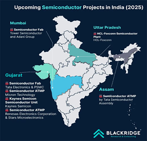
Following the launch of ISM and the introduction of various enabling policies by MeitY, many semiconductor projects are on the anvil (refer to Table 2). These projects would require rigorous monitoring to ensure successful completion within the stipulated timelines. These projects and initiatives have to be ramped up rapidly in both scale and sophistication to meet strategic objectives and global standards.
Table 2. Upcoming Semiconductor Projects in India
| Facility Name | Type | Location | Investment | Partners/Promoters | Expected Commissioning |
| Tata Electronics Fab | Fabrication | Dholera, Gujarat | ₹91,000 crore | Tata + PSMC (Taiwan) | 2026 |
| Micron ATMP Facility | ATMP | Sanand, Gujarat | ₹22,000 crore | Micron + Tata Projects | Early 2025 |
| Kaynes OSAT Facility | OSAT | Sanand, Gujarat | ₹3,307 crore | Kaynes + ISO Tech + Aptos | Mid 2025 |
| CG Power – Renesas
ATMP Unit |
ATMP | Sanand, Gujarat | ₹7,500 crore | CG Power | 2026 |
| Tata OSAT Plant (TSAT) | OSAT | Morigaon, Assam | ₹27,000 crore | Tata Semiconductor Assembly & Test Pvt Ltd | 2026 |
| HCL-Foxconn Fab | Fabrication | Jewar, U.P. | ₹3,706 crore | HCL Group + Foxconn | Late 2026 |
| Micron SEZ | SEZ | Sanand, Gujarat | ₹13,000 crore | Micron Technology | 2025 |
| C-MET Hyderabad Lab | R&D | Hyderabad, Telangana | N/A | MeitY | Ongoing |
| ChipIN Centre (Pan-India) | Training | Multiple Locations | N/A | MeitY + SCL + Industry Partners | Ongoing |
| SicSem Pvt Ltd | Fabrication | Bhubaneshwar, Odisha | ₹2,500 crore | SiCSem Private Limited | 2028 |
Source: “Top Upcoming Semiconductor Projects in India (2025)”, Blackridge Research & Consulting, 30 August 2025.
Source: “Top Upcoming Semiconductor Projects in India (2025)”, Blackridge Research & Consulting, 30 August 2025.
Defence Implications of India’s Semiconductor Push
The Semiconductor Mission is not only technological but also a strategic necessity. Apart from vital national objectives that the ISM seeks to accomplish, the focus on its critical offshoot, i.e., defence implications, is essential. Modern warfare depends on semiconductors for communication, sensing and decision-making. Weaknesses in the supply chain can decide the outcome. India’s dependence on foreign ecosystems exposes it to coercion and supply disruptions.[23]
Semiconductors in Modern Warfighting Systems
Semiconductors underpin C4ISR networks, precision-guided munitions, electronic warfare and autonomous platforms. From BrahMos to drone defence and AI-enabled UAVs, these systems demand advanced processors and specialised devices such as GaN and SiC. Any shortage or compromise could slow India’s Observe-Orient-Decide-Act (OODA) loop, reducing its effectiveness on the battlefield.[24]
Strategic Autonomy and Technology Denial Risks
Export controls under regimes such as the Wassenaar Arrangement and ITAR restrict India’s access to advanced semiconductor technology. Without local fabs, India risks operational paralysis during crises, reliance on subpar imports, weakened deterrence, and even potential strategic collapse.[25] Indigenous capacity is essential to mitigate technology denial.
Civil–Military Fusion as a Force Multiplier
Civil–Military Fusion (CMF) integrates civilian innovation into defence applications. Global powers already benefit by leveraging commercial semiconductor progress for military systems. About 41 of the top 100 global defence firms are US-based, 27 are European, with China rapidly ascending.[26] India can adopt this model to reduce R&D costs, accelerate deployment of advanced electronics, and ensure interoperability between civilian and military AI systems. A chip designed for commercial AI at 14 nm, for instance, can be ruggedised for portable ISR devices.
Secure Supply Chains and Trusted Foundry Requirements
Trusted foundries are vital for defence systems to prevent malicious implants and hardware Trojans. Secure fabrication requires restricted-access fabs, documented supply chains, and verification labs capable of destructive analysis. Relying on imported chips risks espionage and sabotage, even from friendly suppliers.[27]
Significance for Specific Defence Domains
- Aerospace and Space Systems: Satellites need radiation-hardened chips. Dependence on US and European suppliers creates vulnerabilities, especially in crises.
- Naval Combat Systems: Submarines and destroyers rely on fast processors for sonar, radar and fire control. Lack of local production risks slower combat responses.
- Cyber Defence: Hardware security is crucial. Imported chips could hide backdoors that compromise resilience.
- Missile/Air Defence: Hypersonic systems require ultra-fast processors. Import reliance raises the danger of compromise or delay in critical systems.
Enhancing Deterrence through Semiconductor Sovereignty
A self-reliant semiconductor base strengthens deterrence through assured capability and strategic signalling. Indigenous microelectronics ensure operational readiness and technological parity or superiority for projects. This credibility acts as a non-kinetic deterrent, influencing adversaries much like nuclear capability affects strategic calculations.[28]
Blueprint for Defence-Enabled Semiconductor Advancement
As semiconductors become an integral part of the global value chain, all stakeholders should prioritise advancing domestic capabilities. The current trajectory of advancement might play out as a case of ‘too little, too late’. National efforts to build on our strengths and focus on the holistic development of the supply chain are the need of the hour. These efforts would not only secure our national interests, but also serve as a critical defence instrument.
Phase I: Forging Path for Semiconductor Ambitions (2025–2028)
India must embed itself across all stages of the semiconductor value chain by addressing workforce and material gaps. The focus should be on mature nodes like 65/130 nm, with higher ROI and domestic-demand applications. Success hinges on proactive policy funding, streamlined fab and ATMP projects, sustained HR development through global partnerships, and secure, eco-responsible sourcing of raw materials to build a competitive, self-reliant ecosystem.
| Year 2025- 2028 Deliverables |
| National Objectives |
|
| Defence Objectives |
|
Phase II Strategic Expansion and Niche Specialisation (2029–2032)
India will improve existing fabs for greater yields, expand into 28nm+ chips, and pursue niche R&D in GaN, SiC and AI technologies through global partnerships. Build robust IP protection mechanisms via incubators co-located with “Semiconductor Zones” and by diversifying raw material sourcing near clusters. This will ensure resilience, innovation and sustainable semiconductor growth.
| Year 2029- 2032 Deliverables |
| National Objectives |
|
| Defence Objectives |
|
Phase III Core Integration and Atmanirbharta (2033–2036)
Position India as a global semiconductor leader by driving advanced chip design, defence-grade clusters and innovation through public–private collaboration. A reinvested R&D fund will expand CoEs and fuel AI, quantum and materials science. By advancing beyond mature semiconductor nodes, India is poised to climb the global value chain, fortifying supply chain resilience and asserting its leadership in next-generation technologies.
| Year 2033-2036 Deliverables |
| National Objectives |
|
| Defence Objectives |
|
Conclusion
The recently concluded SEMICON India 2025 saw participation from the who’s who of the Global Semiconductor Industry. India unveiled its Vikram 32 chip (a 180nm CMOS processor), modest compared to RAD5545 or the GR740 family of chips, however, it is a vital step in the right direction. India’s semiconductor mission, if implemented with a defence-first lens, can transform its armed forces into technology-resilient warfighting entities. The stakes are existential: in the next high-intensity conflict, the side with the most secure and reliable semiconductor supply chain will dictate tempo, precision and survivability.
India’s semiconductor push represents a rare strategic convergence—an industrial initiative that is also a force multiplier for national defence. If executed with discipline, foresight and defence-sector anchoring, it can achieve what nuclear self-reliance did in the late 20th century: secure India’s strategic autonomy in an era where wars will be won as much in silicon as on the battlefield. The choice is binary—remain a dependent consumer in a fragmented global supply chain, or emerge as a trusted, sovereign and indispensable semiconductor power that underwrites both economic growth and military supremacy.
Cdr Gourav Yadav is presently undergoing the 32nd Naval Staff and Technology Management Course (NSTMC) at Naval War College, Goa.
[1] Chris Miller, Chip War: The Fight for the World’s Most Critical Technology, New York, Scribner, 2022.
[2] Shayesta Nishat Ahmed, “India’s Strategic Push for Semiconductor Manufacturing”, Issue Brief, Manohar Parrikar Institute for Defence Studies and Analyses (MP-IDSA), 23 September 2024.
[3] Sarat Chinta, “India’s Semiconductor Growth: Opportunities, Comparisons, and the Case for Local Manufacturing”, SSRN, 29 January 2025..
[4] “Annual Report 2024–25”, Ministry of Electronics and Information Technology, Government of India, pp. 76–77.
[5] S. Ezell, “Assessing India’s Readiness to Assume a Greater Role in the Semiconductor Ecosystem”, Information Technology and Innovation Foundation, 14 February 2024.
[6] “Critical Determinants of Civil-Military Fusion in India”, Centre for Air Power Studies, 10 April 2024.
[7] “Emerging Trends in the Global Semiconductor Industry”, RAND Corporation, 2020.
[8] Tim [D-OH-13] Rep. Ryan, “Text – H.R.4346 – 117th Congress (2021-2022): CHIPS and Science Act”, 9 August 2022.
[9] “Securing the Microelectronics Supply Chain: Four Policy Issues for the U.S. Department of Defense to Consider”, RAND Corporation, 2022.
[10] Sujai Shivakumar et al., “The Pillars Necessary for a Strong Domestic Semiconductor Industry”, Center for Strategic and International Studies (CSIS), 1 May 2022.
[11] Ibid.
[12] Konark Bhandari, “The Geopolitics of the Semiconductor Industry and India’s Place in It”, Carnegie Endowment for International Peace, 2023.
[13] Akhil Thadani and Gregory C. Allen, “Mapping the Semiconductor Supply Chain: The Critical Role of the Indo-Pacific Region”, Center for Strategic and International Studies, 2023.
[14] Rajiv Kumar, “The US-China Chip War and Prospects for South Korea-India Semiconductor Cooperation”, The Journal of Indian and Asian Studies, Vol. 4, No. 2, 2023.
[15] Mikko Huotari, “Mapping China’s Semiconductor Ecosystem”, Mercator Institute for China Studies (MERICS), Berlin, 2023.
[16] William A. Reinsch, Emily Benson and Aidan Arasasingham, “Securing Semiconductor Supply Chains: An Affirmative Agenda for International Cooperation”, Center for Strategic and International Studies (CSIS), 2022.
[17] “Semiconductor Push: India Hosts 20% of World’s Chip Design Engineers; Consumption Set to Cross $120 Billion by 2030”, The Times of India, 2 September 2025.
[18] “Annual Report 2024-25”, Ministry of Electronics and Information Technology, Government of India, p. 82.
[19] “Assessing Systemic Strengths and Vulnerabilities of China’s Defense Industrial Base”, RAND Corporation, 2022.
[20] “2023 Global Top 10 Wafer Manufacturers’ Production Capacity and Output”, EnergyTrend, 2023.
[21] Eleanor Olcott et al., “China Struggles to Break US Chip Design ‘Chokehold”’, Financial Times, 24 October 2024.
[22] Brian Martin, “Supply Chain Interdependence and Geopolitical Vulnerability”, RAND Corporation, 2023.
[23] Sujai Shivakumar and Charles Wessner, “Semiconductors and National Defense: What Are the Stakes?”, CSIS, 8 June 2022.
[24] Dagmar van Westen, “Disrupting Disruptions: Enhancing Supply Chain Resilience—Lessons from the US Air Force”, Annals of Operations Research, July 2025.
[25] Laura H. Baldwin et al., “Supply Chain Interdependence and Geopolitical Vulnerability: The Case of Taiwan and High-End Semiconductors”, RAND Corporation, 2023.
[26] “The SIPRI Top 100 Arms-Producing and Military Services Companies in the World, 2023”, Fact Sheet, Stockholm International Peace Research Institute, December 2024.
[27] James Mulvenon, “The Trusted Foundry Program and the Role of Microelectronics in U.S. National Security”, RAND Corporation, 2013.
[28] Harsh V. Pant, The Routledge Handbook of Indian Defence Policy: Themes, Structures and Doctrines (2nd edn), Taylor & Francis Group, 2020.
[29] Ulupi Borah, “India’s Semiconductor Ecosystem in Joint Warfighting: Exploring Strategic Collaboration in the Indo-Pacific”, Synergy, Vol. 3, No. 2, August 2024.