Computational Resource Control: The 2025 US AI Framework
- February 25, 2025 |
- Issue Brief
Summary
The new US export control regulation for Responsible AI Diffusion uses Total Processing Performance (TPP) to measure restrictions. It focuses AI capabilities in Tier 1 countries while redirecting the GPU market to US-preferred geographies. Tier 2 countries face limitations on US-controlled GPU access, needing bilateral synchronisation with US export policies for more compute power. Ambiguities in methodologies and variables for country-based allocations and NVEUs may pose implementation challenges.
Introduction
The Biden-Harris administration introduced the Framework for Artificial Intelligence Diffusion (heretofore, ‘the Framework’) on 15 January 2025, a significant expansion of US control over advanced computing resources, particularly Graphic Processor Units (GPUs), in the global AI landscape. The policy was initiated with an explicit aim of protecting US national security by maintaining ‘its leadership in the science, technology, engineering, and manufacturing sectors, including foundational technology that is essential to innovation’.[i] The framework inserts new control mechanisms in the Export Administration Regulations (EAR), administered by the Bureau of Industry and Security (BIS), which is the agency under the US Department of Commerce. It establishes a multi-tiered licensing classification system and precise computational resource allocation metrics based on Total Processing Performance (TPP), graded differently for different countries.
The Framework, in simpler terms, hinges on two parameters for classification and implementation of export controls: a country classification system for access control and a computational resource allowance based on fixed TPP allocation. This Brief examines the specific country categorisations under the new licensing regime and analyses the technical parameters used to determine computational resource thresholds. Understanding these components is crucial for grasping how the framework reshapes global access to advanced AI computing capabilities, particularly as the policy seems to maintain its force through the new Trump administration’s cull of policies (including those on AI) made by the erstwhile Biden-Harris administration.
The New Hierarchies of Access
The Framework has introduced a three-tier structure for various countries, based on which TPP allocations will apply.
- Tier 1 includes 18 states which are considered close allies and important semiconductor supply chain partners of the US, and are listed under Supplement no. 5 of Part 740 of the BIS.[ii] These countries are those that have export control mechanisms deemed trustworthy, and are similarly aligned in terms of the strategic technological transfer, with the US. These countries have access to streamlined and relatively unrestricted GPU access through the Artificial Intelligence Authorization (AIA) exception, as long as the entity importing them is headquartered or has a parent company in a Tier 1 country itself.
- Tier 2 countries encompass a vast majority of countries which import GPUs from the US. A large chunk of the changes in the Framework pertain to this tier, and the introduced exceptions, quotas and rules that may lead to differentiation in TPP allocations are mostly applicable herein. This category hosts countries with varied relationships and status vis-à-vis Singapore, a trusted US ally, is a tier 2 country just like Yemen, which is known to have bombed US tankers.[iii] These countries have access to a base cumulative TPP of 790,000,000 as one-time allowance, outside of Data Centre Validated End Users (DC-VEU) allocations, Low Processing Performance exemptions and retail allowances. These countries may negotiate an increase in their TPP allocations with the US on a bilateral basis, which will be granted to them on a case-by-case basis based on how much they agree to align their security and export control to US, through assurances and agreements. India is also included in this tier.
- Tier 3 includes Macau and countries which are part of the arms embargoed countries listed under D:5 of the Supplement No. 1 to Part 740 of the EAR. Exports of chips covered under the Framework are nearly banned herein[iv].
Beyond the country-based allocations, these tiers are also relevant for a second layer of export control, which is imposed on DC-VEUs. The framework bifurcates DC-VEU into two: Universal VEUs (UVEU) and National VEUs (NVEU). The allocations herein are based on the tier of the country the company applying for specific VEU is from, where the Data Centre it is establishing is, and the relative scale of the DC.
- UVEU status can be granted to companies that have their headquarters or ultimate parent in a Tier 1 country, and meet the requisite compliance standards with adequate level of stringency. Companies that qualify for UVEU status may have relatively unimpeded access to GPU imports, but will have to follow strict security requirements across their supply chain. Additionally, UVEUs need to adhere to the following requirements:
- At least 75 per cent of the company’s total computing power is in Tier 1 countries only.
- At any given time, the company’s compute in a single tier 2 country should not exceed 7 per cent of its total compute.
- For US-based UVEU, 50 per cent of its total AI compute MUST be within the US itself.
It should be noted that a company with UVEU status can deploy in any of the Tier 1 or Tier 2 countries without seeking separate authorisation for each location, as long as they adhere to the aforementioned compute percentages.
- NVEU status is available to companies in both Tier 1 and Tier 2 countries, to import GPUs for Data Centres to be established in either Tier 1 or Tier 2 countries only. A company with NVEU status will have more freedom in terms of locations to establish data centres. They have separate allocations for import of GPUs, which does not add to national allocation limits. However, an NVEU authorisation for import of GPUs applies only to one country, i.e., if a company wishes to establish a data centre in another country, it will have to apply for another authorisation for the new location.
The GPU allocation for NVEUs for each company on per country basis is shown in Table 1.[v]
Table 1: Cumulative GPU Allocation on per-company per-country basis (2025–2027)
| Year-Quarter | TPP Allocation (Cumulative) |
| 2025 Q1 | 633,000,000 |
| 2025 Q2 | 949,500,000 |
| 2025 Q3 | 1,266,000,000 |
| 2025 Q4 | 1,582,500,000 |
| 2026 Q1 | 1,899,000,000 |
| 2026 Q2 | 2,690,250,000 |
| 2026 Q3 | 3,481,500,000 |
| 2026 Q4 | 4,272,750,000 |
| 2027 Q1–4 | 5,064,000,000 |
Source: Export Administration Regulations (EAR), Bureau of Industry and Security.
These numbers, however, are not additive, but cumulative, i.e., the TPP allocation for each quarter includes total allocations for previous quarters. Therefore, an NVEU can import around 5 million TPP for each country by the end of 2027.
Notably, the Framework does provide certain allowances for imports of GPUs that do not count towards national and VEU allocations. For instance, countries are allowed to import up to 26,900,000 per customer per calendar year as part of the Low Processing Performance (LPP) exception. The LPP exception exists for small-scale deployments that do not pose a significant national security risk to the US. LPP exception allows entities to not require full license for import of GPUs, but they need to inform BIS of the purchase. Another exception is retail purchases of GPUs (for purposes such as gaming systems primarily), which are not under strict control by the Framework norms. It should be noted that neither of these exceptions are available for Tier 3 countries.
TPP Formula Variations from Variable Interpretation
As can be seen above, TPP is the essential metric for establishing how much computing power can be imported by a country or company according to the Framework. Several studies that have followed the regulation have attempted to clarify these regulatory controls through analyses that have tried to translate the TPP framework into practical terms, primarily through examples of affected GPU quantities.
These interpretations, whether accompanied by detailed calculation methodologies or not, have established a chip-centric approach to understanding TPP thresholds and their implications for AI development capabilities. For instance, RAND Corporation’s analysis uses the H100 SXM chips (FP16 Tensor core) specifications to calculate TPP in terms of ~50,000 chips,[vi] while a report by The Diplomat establishes these limits in terms of ~50,000 A100 chips[vii] to define 790,000,000 TPP that is allotted to Tier 2 countries.
This equivalence in chip quantities presents a notable inconsistency, as the H100 and A100 possess substantially different computational capabilities. While both analyses arrive at approximately 50,000 chips to reach the 790 million TPP threshold, their underlying calculations raise questions about methodology choices. Particularly, while these studies provide some computational details, they often do not justify their choice of non-sparsity TFLOPS (Tera Floating Point Operations per second) values in their calculations.
Typically, TPP calculation for a chip is based on the following formula:
TPP = TFLOPS x Bit-length
Where TFLOPS represents a system’s capability to do 10¹², i.e., one trillion, floating-point calculations per second, and bit-length represents how many binary digits are used to represent an unsigned integer as a binary number for these operations. Higher bit-length means higher degree of precision, but at the same time also raises the amount of time and computing required to carry tasks. This is the formula used by some of the researchers to calculate the number of chips, by dividing the TPP value of a chip with the total TPP value allocated (790 million in this case).
RAND, for instance, does the calculation based on values mentioned in NVIDIA product brochure for H100 chips[viii] (assumed to be 990 TFLOPS in non-sparsity), i.e.,
TPP per chip for H100 SXM (FP16 Tensor core) = 990 x 16 = 15,840
Therefore, number of chips that make up to 790 million TPP is
790,000,000 ÷ 15,840 = 49,873.73 chips
Based on these calculations, projected figures for NVEU allocations on per-company per-country basis are shown below:
Figure 1. Cumulative Computing Power Limits for NVEU Authorisations (2025–2027)
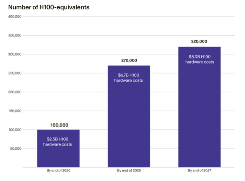
Source: Understanding the Artificial Intelligence Diffusion Framework, RAND Corporation, January 2025, p. 4.
It is important to note that these figures are based on non-sparsity compute. Non-sparsity means a chip will process ALL the data, which raises inefficiency because certain filled data points it must process may be unnecessary. To filter out this unnecessary data, modifications are made to a chip, through hardware optimisations and/or software based model training that introduce techniques which might skip the unnecessary data. This feature, known as Sparsity, increases the efficiency and maximises processing power. Per the industrial standards, chip processing numbers with sparsity are ideally considered to be double of those non-sparsity. Per the NVIDIA product specifications, for instance, the computation power of H100 SXM GPUs with sparsity is 1979 TFLOPS.
This is significant, since BIS has expressed the calculation of TPP differently. According to the Supplement 1 to Part 774 of the EAR, the TPP calculation formula is
TPP = 2 x MACTops x Bit-length
Wherein MACTops (Multiply-Accumulate Operations per Second) is a measure of computational performance, where each MAC operation consists of two operations: one multiplication and one addition. In essence, 2 TFLOPS make 1 MACTops operation, which means
TPP = 2 x MACTops x Bit-length = TFLOPS x bit-length
More importantly, the values in consideration for TPP must be the maximum value theoretically possible. The technical notes provided with the EAR formula specifically mentions how the rate of ‘MACTops’ must be assumed to be the highest value the manufacturer claims ‘in annual or brochure’.[ix] For this, the values considered must be when the chip’s processing power is more efficient and maximised, i.e., with sparsity (which is a contradiction to RAND’s consideration of non-sparsity values).
Using these considerations, another interpretation of the value of TPP per chip for H100 chips could be
TPP per chip for H100 SXM (FP16 Tensor core) = 1,979 x 16 = 31,664
Therefore, the number of chips that make up to 790 million TPP is
790,000,000 ÷ 31,664 = 24,949.5 chips
Similarly, the NVEU allocations at per-company per-country basis are:
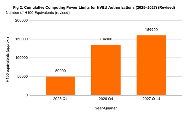
Source: Author’s own tabulation based on revised formula.
The variation in these numbers represents a widespread ambiguity and confusion regarding the parameters of calculation of how much GPU allocation is allowed for exports. The TPP framework, while designed to establish clear regulatory boundaries, suffers from inconsistent variable interpretation that leads to conflicting calculations. The discrepancy between RAND’s approach using non-sparsity values and the apparent regulatory intention of using “theoretical maximum” performance metrics demonstrates a fundamental challenge in implementing these controls. This ambiguity not only creates confusion for stakeholders attempting to understand compliance requirements but may also result in significantly different practical limitations depending on which calculation method prevails.
Strategic Implications and Future Trajectories
The TPP framework presents substantial challenges for India’s AI ambitions, particularly its goal of a 10,000 GPU supercomputer by 2025.[x] These regulations further constrain the already conservative estimates for the IndiaAI mission, highlighting the critical importance of the India Semicon Mission for indigenous development. However, domestic GPU manufacturing faces significant technological and capital investment hurdles, with India being years behind the curve compared to established semiconductor powers like the US, South Korea and Taiwan. Though India’s classification in the General VEU category alongside China comes with broader allowances, it still indicates continued US caution that may limit India’s ability to secure maximum TPP allocations.
The tiered regulatory structure will likely concentrate large-scale AI clusters within Tier 1 countries, effectively redirecting market demand to geographies aligned with US strategic interests. Rather than creating a disadvantage for American GPU manufacturers, this framework reinforces dependence on US markets while maintaining competitive advantages in trusted jurisdictions. Nevertheless, this may mean that the market manufacturers may not publish inflated values for the GPU speed (even in non-sparsity), which may also help in raising threshold for exports to Tier 2 markets.
Meanwhile, China’s complete exclusion from advanced computing resources remains questionable given its demonstrated ability to utilise shell companies for procurement.[xi] Despite NVEU allocations and import limitations, measures may be only partially effective against China’s adaptability, as evidenced by achievements like the DeepSeek model developed with comparatively limited resources.
For Tier 2 countries, the NVEU mechanism represents the primary pathway for accessing advanced GPUs, necessitating greater private sector involvement in developing national AI capabilities within regulatory constraints. Fortunately, current computing requirements for most Tier 2 countries remain below allocated thresholds, providing some breathing room for immediate needs. However, the lack of clarity in TPP calculations introduces significant confusion into the regulatory landscape, complicating compliance efforts and strategic planning while potentially leading to inconsistent enforcement and uneven competitive conditions across markets.
The implications of these regulations extend beyond immediate access limitations to reshape the global AI development landscape. By directing advanced AI capabilities to preferred geographies, the US aims to maintain technological leadership while minimising potential security risks. However, this approach may inadvertently accelerate indigenous development efforts in restricted countries, potentially fragmenting the global AI ecosystem along geopolitical lines. For countries like India, navigating these constraints will require balancing international partnerships, domestic innovation initiatives and creative approaches to maximising computing resources within regulatory boundaries.
Views expressed are of the author and do not necessarily reflect the views of the Manohar Parrikar IDSA or of the Government of India.
[i] Bureau of Industry and Security, ‘Framework for Artificial Intelligence Diffusion’, Federal Register Volume 90 No. 9. January 15, 2025.
[ii] “Supplement No. 5 to Part 740 – Artificial Intelligence”, Title 15, Subtitle B, Chapter VII, Subchapter C, Part 740, U.S. Code of Federal Regulations, Bureau of Industry and Security (BIS), U.S. Department of Commerce, 4 February 2025.
[iii] “2025 AI Diffusion Export Controls: Microsoft Regulatory Capture, Oracle Tears“, SemiAnalysis, 15 January 2025.
[iv] While China may not be able to import any chips through the framework normally, it is allowed restricted imports as part of General Validated End User (VEUs) only for specific civilian purposes. India has also been granted access through this path, but India is allowed civilian as well as limited military applications.
[v] U.S. Department of Commerce, Bureau of Industry and Security, “Export Administration Regulations (EAR)”, Federal Register, Vol. 90, No. 9, 15 January 2025.
[vi] Lennart Heim, “Understanding the Artificial Intelligence Diffusion Framework”, RAND Corporation, January 2025.
[vii] Fatih Oktay, “The US AI Diffusion Framework: Global Implications and Unintended Consequences”, The Diplomat, 31 January 2025.
[viii] “NVIDIA Tensor Core GPU Datasheet”, NVIDIA.
[ix] ‘Annual’ here refers to annual reports, which are formal documents that companies publish yearly on aspects such as product claims. ‘Brochure’ refers to product marketing materials. The numbers reflected in these documents are often the ‘idealised’, or rather theoretically possible compute value possible in laboratory conditions.
[x] Charlotte Trueman, “Indian Government Launches $1.2bn IndiaAI Mission, Plans 10,000 GPU Supercomputer“, Data Center Dynamics, 8 March 2024.
[xi] Cheng Ting-Fang, “How China’s Tech Ambitions Slip Through the U.S. Export Control Net”, Nikkei Asia, 20 October 2023.